

AST
About Advanced Substrate Technologies Pte. Ltd.
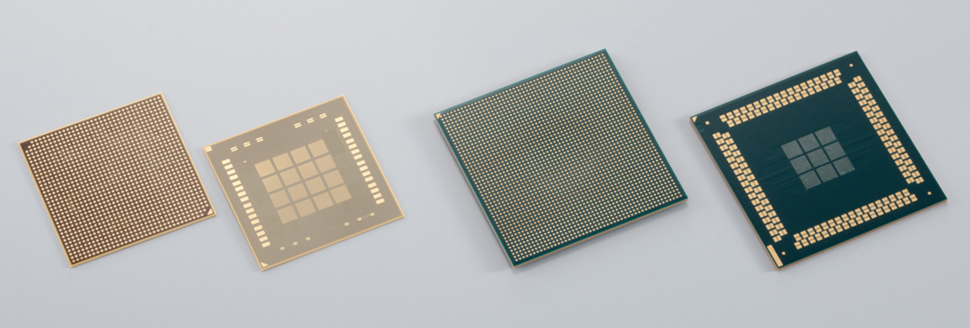
We are a Singapore-based subsidiary of TOPPAN Holdings Inc., a Japanese pioneer in printing technologies and a leading supplier of high-quality Flip Chip Ball Grid Array (FC-BGA) substrates. We are the first factory in Singapore to pioneer the manufacturing of high-end FC-BGA substrates used in cutting-edge semiconductor products such as network switches and artificial intelligence (AI)/machine learning (ML) devices.
Additionally, our facility will conduct research and development (R&D) aimed at advancing substrate technologies to meet the evolving performance requirements of future products in these domains. Broadcom Inc., a global technology leader specializing in semiconductor design, enterprise software, and security solutions, is also actively supporting the establishment of this state-of-the-art manufacturing facility in Singapore.
Our Research & Development
Do you thrive on developing groundbreaking technologies that lead to amazing new products? Are you meticulous and committed to excellence, always aiming for extraordinary results? Come see what you can achieve with AST R&D team! We believe that new ideas swiftly become remarkable products. With your passion and dedication, there’s no telling the impact you’ll make.
Company Overview
Our AST R&D team is on a mission to transform AI and develop groundbreaking hardware. We’re creating innovative solutions for tighter, quicker, and more dependable integration of processing and memory, moving beyond the limitations of current substrate technologies. We leverage cutting-edge semiconductor processing technologies, including Chemical Mechanical Planarization, to produce high-performance substrates with 10x increase in interconnect density, paving the way for packages with up to a trillion transistors.
Job Responsibilities
Package Architecture, Co-Design & Optimization
Package design & Integration
Technical Skills Strong experience in one or more of the following tools:
Perform any other ad-hoc duties as assigned by the Manager, as required to support the team and organizational goals. |
Job Requirements
Required Qualifications:
- Bachelors and 8+ years or Masters degree and 6+ years or PhD and 3+ years of related experience.
- BS/MS/PhD in Electrical Engineering (Preferred), Mechanical Engineering, Materials Science, or related field.
- Extensive hands-on experience in advanced IC packaging for advanced silicon nodes.
- Proven experience using simulation tools for complex engineering problems, ideally in Signal integrity.
- Strong understanding of high layer count, large body, flip chip BGA packaging technology.
- Proficiency in ANSYS HFSS, SI/PI, Signal integrity.
- Strong analytical, problem-solving, and communication skills. Ability to work both independently and as part of a team.
- Proven ability to drive NPI through HVM with strong cross-functional leadership.
- Excellent communication, documentation, and customer-facing skills.
Location & Commitments
- Premises located in 9 Pesawat Drive, Singapore 619607
- Permanent, full-time role working 40 hours per week
Contact us to apply
If you believe you possess the qualifications for this position, please submit your resume and cover letter to our HR team at hr_career@ast-sg.com.
Why Join Us
- Work on cutting-edge projects in a growing field.
- Collaborative and innovative environment.
- Competitive compensation and benefits.
- Opportunities for professional development.
Closing Statement
AST is dedicated to creating a workplace that is diverse, equitable, and inclusive, where every employee feels appreciated, respected, and empowered to share their unique perspectives.
Connect With Us!
Find out our latest happenings in social media:


To apply for this job email your details to hr_career@ast-sg.com