Denounce with righteous indignation and dislike men who are beguiled and demoralized by the charms pleasure moment so blinded desire that they cannot foresee the pain and trouble.
Read More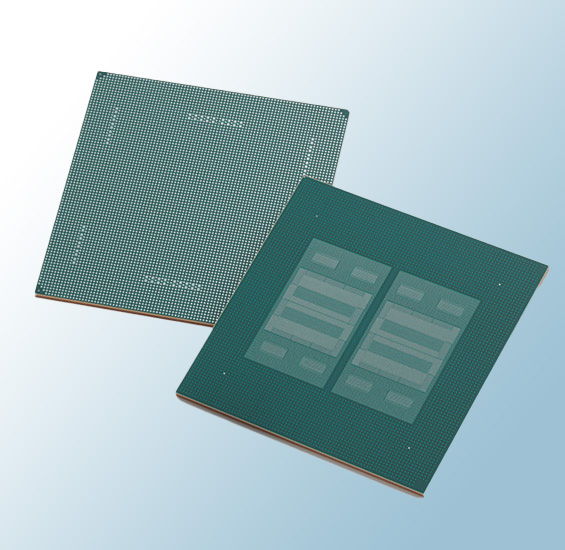
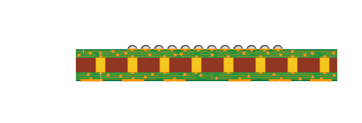
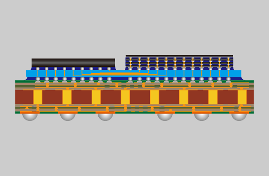
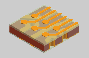
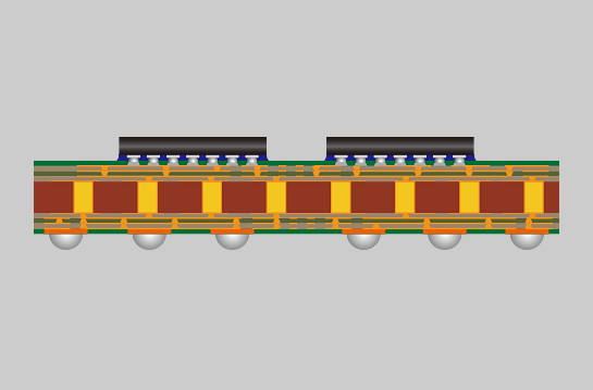
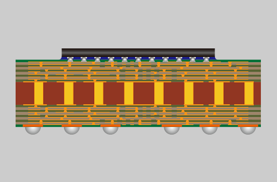
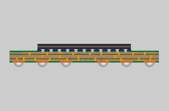
Core Process
Drill holes in the core material and plate it with copper. Then remove the copper except for a circuit pattern area.
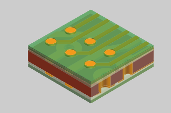
Build-up processing
Expose a circuit pattern to directly form circuit with copper plating. Repeat this treatment and laminate (build up)
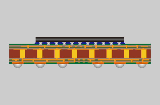
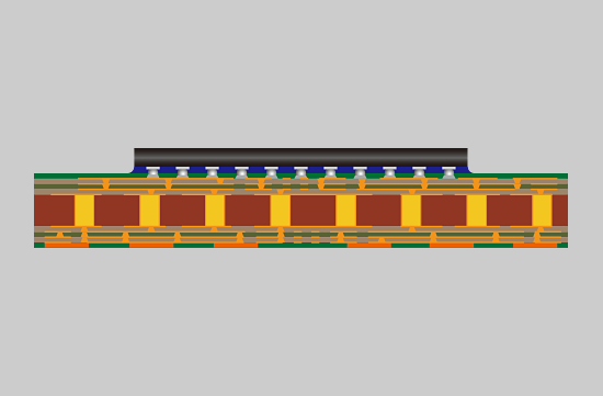
Outer layer Process
After applying solder resist, place solder bumps where LSI chips (die) will be mounted. After cutting into each pieces, inspect appearance and electric characteristics.

Network device
(ASIC)

Server / PC
(CPU)

AI Processor
(AI)

Automotive
(Infotainment / ADAS)

Home Game Console
(SoC)

Graphic Processing Unit
(GPU)
FC-BGA
FC-LGA
Multi-chip FC-BGA
Ultra-multilayer FC-BGA
Coreless FC-BGA